AC and DC Characteristics of Operational Amplifier
Operational Amplifier
Op-amps or operational amplifiers are one of the fundamental components of analogue electronic circuits. In this article on the fundamentals of operational amplifiers, we will learn operational amplifiers devices with all the characteristics needed for essentially perfect DC amplification. To execute mathematical operations including addition, subtraction, integration, and differentiation as well as signal conditioning and filtering, op-amps are frequently utilized.
Operational amplifiers, or op-amps for short, are voltage-amplifying devices that are primarily intended to be used with external feedback components like resistors and capacitors between their input and output terminals. The term "Operational Amplifier" originated from the fact that the amplifier may carry out a variety of activities thanks to the several feedback topologies, whether resistive, capacitive, or both. The amplifier's "operation" or final function is determined by these feedback components.
At its essence, an operational amplifier is a three-terminal component with two high-impedance inputs. One of the inputs is the inverting input, which is designated by a "minus" or negative sign ( – ). The non-inverting input, often known as the second input, is indicated by a plus sign (+).
Further, the third terminal, which can supply or sink a voltage or current, represents the operational amplifier's output port. The output of a linear operational amplifier is equal to the input signal's magnitude times the amplifier gain (A), also known as the amplification factor. There are two main types of operational amplifier gain, depending on the properties of the input and output signals.
AC Characteristics
One should must be familiar with ac characteristics like frequency response and slew-rate for tiny signal sinusoidal (AC) applications. Let’s discuss each of them:
1. Frequency Response:
Gain magnitude and phase angle will fluctuate due to differences in operating frequency. The frequency response describes how the gain of the op-amp reacts to various frequencies. In other words, if an op-open amp's loop gain is 90 dB with a DC signal, that gain should stay at 90 dB through audio and onto high radio frequencies. When a specific frequency is achieved, the op-amp gain diminishes (rolls off) since it does so at higher frequencies. The corresponding circuit of the op-amp must have a capacitive component.
For an op-amp with a single break (corner) frequency, one capacitor C may be used to represent all of the effects of the capacitors. Figure given below depicts a modified version of the lower frequency variant with capacitor C at the output.
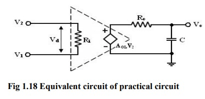
One pole and one -20dB/decade are attributed to R0C. From the above figure, With a single corner frequency, we may determine the open loop voltage gain of an op-amp.
The op-higher amp's 3 dB frequency or corner frequency is f1. It is possible to write the open loop voltage gain's magnitude and phase angle as follows: The properties of magnitude and phase angle:
1. The gain's magnitude for frequency f f1 is 20 log AOL in db.
2. The gain is 3 dB lower at frequency f = f1 than the AOL value in dc. Corner frequency is used to describe this frequency, f1.
3. The fade-off for f>> f1 is at a rate of -20dB/decade or -6dB/decade.
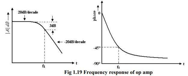
The phase angle at frequency f = 0 is determined by the phase characteristics to be zero. Phase angles range from -45degree (lagging) at corner frequency f1 to -90degree (infinite frequency). It indicates that an op-amp may have a maximum phase change of 90degree when it has a single capacitor, or C. Whereas the decade beyond the corner frequency is seen to have infinite frequency, the decade immediately below the corner frequency is thought to have zero frequency.
2.Circuit Stability:
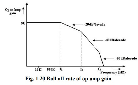
A circuit or network is considered to be stable if the output of a linked circuit or set of connected circuits reaches a particular value in a finite amount of time. A system is deemed unstable if its o/p increases with time as opposed to stabilizing. In actuality, an unstable system's output keeps rising until it crashes. The unstable system must be made stable because it is impractical. Whenever the network is to be put to a practical test, the stability criteria (gn) are applied. Theoretically, Bode graphs are always used to check a system's stability.
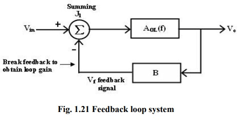
Bode graphs of magnitude vs frequency and phase angle versus frequency are contrasted. The block diagram may be used to illustrate any structure whose stability has to be determined.
The forward block is the one between the output and the input, while the feedback block is the one between the output and the f/b signal. Each block's content is referred to as its transfer frequency. We showed it in Fig. by using AOL (f), which is provided by
AOL (f) = V0 / Vin if Vf = 0 ----- (1)
where AOL (f) = open loop voltage gain.
The closed loop gain Af is given by AF = V0/Vin
= AOL / (1+(AOL ) (B) ----(2)
Here, B = gain of feedback circuit. B is a constant if the feedback circuit only consists of resistive components.
The system's stability may be evaluated in the following ways once the phase angle Vs frequency and magnitude Vs frequency charts have been created.
1. Case 1
What is the phase angle when the magnitude of (AOL) (B) is 0dB (or) 1?
A stable system has a phase angle higher than 180. For some systems, the magnitude might never be zero, in such case approach 2 must be used.
2.Case 2
When the magnitude of (AOL) (B) is 0dB (or) 1, what is the phase angle?
The system is stable if the phase angle is greater than -180 and the magnitude is -ve dB. However, in some systems, the phase angle can approach -180, hence in these cases, case 1 must be used to assess the stability of the system.
DC Characteristics of OP-Amp
Op-amp inputs receive current from the source and react to it differently.
Voltage brought on by a transistor mismatch.
DC output voltages are,
- Input offset -current
- Input offset voltage
- Input bias current
- Thermal drift
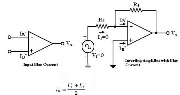
Input bias current:
The op-input is made up of differential amplifiers, which can be made of BJT or FET.
We reasoned that the base currents entering the non-inverting and inverting terminals (IB+ & IB-) were constant as no current is drawn from the input terminals of an ideal op-amp.
IB+ and IB- are not exactly equal despite the fact that both transistors are identical because of an inherent imbalance between the two inputs. The input bias current IB is described by manufacturers.
This is wholly unsuitable in applications where output levels are measured in mV. The compensation resistor Rcomp, which has been inserted between the non-inverting input terminal and ground as indicated in the figure below, can be used to make up for this.
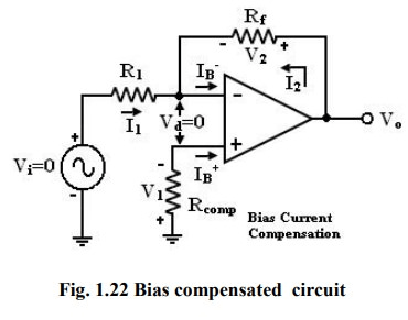
Current IB+ passing via the compensating resistor Rcomp, followed by KVL, to yield
Vo = V2 – V1 --------- (1)
By choosing the right value for Rcomp, V2 and V1 may be canceled, leaving Vo at 0. Rcomp's value is calculated as
IB+ = V1/Rcomp ------------ (2)
Voltage is present at node "a." (-V1). due to the non-inverting input terminal's voltage (-V1). Thus, if Vi = 0, we have,
I1 = V1/R1 -------------- (3)
I2 = V2/Rf -------------- (4)
Vo should equal zero (Vo = 0, Vi = 0) as compensation. V2 = V1 according to equation (3). such that,
I2 = V1/Rf --------------(5)
IB- = I2 + I1 =( V1/Rf ) +(V1/R1) = V1(R1+Rf)/R1Rf ------------------ (5)
Take IB- = IB+ and using equation (2) & (5) we get
V1 (R1+Rf)/R1Rf = V1/Rcomp
Rcomp = R1 || Rf --------------- (6)
So, the compensating resistor, Rcomp, should be equal to the parallel combination of resistors R1 and Rf in order to account for bias current.
Input offset current:
If the bias currents IB+ and IB- are equivalent, bias current correction will function thus identical input transistors are not possible. There will inevitably be some minor
|Ios| = IB+-IB- ---------------- (7)
The offset current Ios for BJT op-amps is 200nA, whereas it is 10pA for FET op-amps. When Vi = 0, offset current will still result in an output voltage even with bias current adjustment.
V1=IB+Rcomp -------(11)
I1=V1/R1-------(12)
KCL at node A gives the final one,
I2=(IB— -I1)---(13)
Again V0 = I2 Rf – V1---(14)
Vo = I2 Rf - IB+ Rcomp----(15)
Vo = 1M Ω X 200nA---(16)
Vo = 200mV with Vi = 0
According to equation (16), by keeping the feedback resistance low, the offset current may be reduced.
- Unfortunately, R1 needs to be kept big in order to get high input impedance.
- The feedback resistor Rf needs to be high if R1 is big. to achieve a justifiable profit.
- The T-feedback network is an effective remedy. This will enable high feedback resistance while maintaining low ground resistance (in dotted line).
- The T-network generates a signal of feedback as if it were a single feedback resistor.
Input offset voltage:
Despite the adoption of the aforementioned compensatory procedures, it is discovered that the output voltage [Vo =0 with Vi= 0] may still not be zero with zero input voltage. As a result of inherent imbalances inside the op-amp, this occurs, and the output (Vo) may need to be set to zero by applying a little voltage to the input wire.
Input offset voltage Vos is the name of this voltage. This is the input voltage that must be provided in order to set the output voltage to zero (Vo = 0).
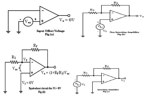
Let's calculate the Vos at the inverting and non-inverting amplifiers' outputs. Figures (b) and (c) become identical to the figure if Vi = 0 to (d).
Total output offset voltage:
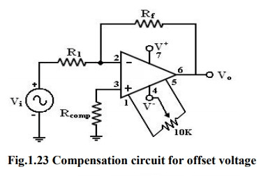
The amount of the total output offset voltage VOT may be different from that of the output offset voltage brought on by input bias current (IB) or input offset voltage alone (Vos). This is because IB and Vos might have either a positive or detrimental effect on the ground. Due to this, many operational amplifiers (op amps) contain offset compensation pins to cancel the offset voltage, providing the maximum offset voltage at the output of an inverting and non-inverting amplifier (figures b, c) without the need for any compensation mechanism. Between pins 1 and 5 of the offset null, insert a 10K potentiometer. The wipes were connected to the negative supply of pin 4. The placement of the wipes is changed to eliminate the offset voltage.
When the op-amps that are offered (below) lack these offsets, outputs, external balancing procedures are employed.
VOT= (1+Rf/R1)VOS+RfIB
With Rcomp, the total output offset
VOT= (1+Rf/R1)VOS+RfIOS